
 Mobile
Repairing Tools
Mobile
Repairing Tools
 Touch/Glass/OCA
Glass
Touch/Glass/OCA
Glass Stencils &
IC
Stencils &
IC OCA Machine &
Parts
OCA Machine &
Parts Mobile
Accessories
Mobile
Accessories Software
 OCA
Sheets &
Polarizers
OCA
Sheets &
Polarizers
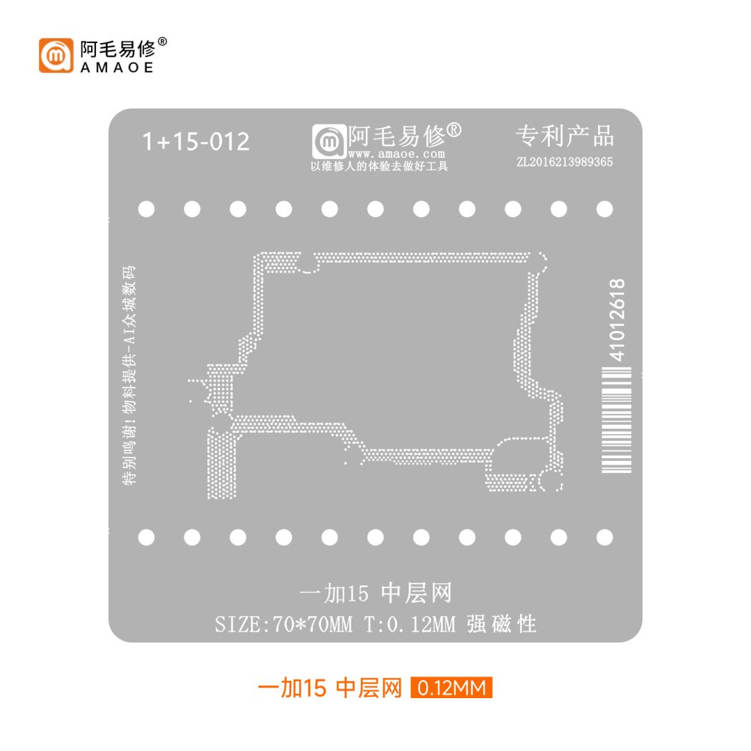
AMAOE 1+15-012 ONE PLUS 15 STENCIL
AMAOE 1+15-012 (OnePlus 15 Series) BGA Reballing Stencil
The AMAOE 1+15-012 is a master-grade BGA reballing stencil meticulously customized for chip-level diagnostics and board repairs on the OnePlus 15 series flagship hardware platforms. Utilizing ultra-hard, imported Japanese steel and precision anti-clog micro-apertures, this stencil offers unparalleled accuracy for advanced mobile technicians dealing with dense logic board trace failures, thermal stress damage, and component swaps on cutting-edge smartphone chipsets.
Product Specifications & Technical Overview
| Attribute | Specification Details |
| Brand | AMAOE (Original Equipment Manufacturer) |
| Model / Part Number | 1+15-012 (OnePlus 15 Dedicated Series) |
| Application Scope | Chip-level micro-soldering, motherboard rework, BGA reballing |
| Target Device Ecosystem | OnePlus 15 / OnePlus 15 Pro / OnePlus 15 Ultra variants |
| Material Build | Premium imported high-tensile Japanese SUS301 Stainless Steel |
| Gauge Thickness | 0.12mm (Industry gold standard for uniform solder paste volume) |
| Manufacturing Method | Ultra-fine CNC Laser Chemical Etching |
| Aperture Geometry | Square openings with micro-rounded corners (Stepped release profile) |
| Thermal Durability Limit | Continuous safe operating tolerance up to 450°C |
| Surface Finish | Electro-polished matte anti-glare, scratch-resistant coating |
Comprehensive Feature Analysis
1. Formulated Specially for Next-Gen Architectures
The 1+15-012 is mapped directly to the highly consolidated architectural layout of contemporary premium mobile chipsets. It accommodates the extremely tight pin-pitches (0.2mm - 0.35mm) found on the principal processing units, power modules, and baseband chips used by high-tier devices.
2. Advanced Square-Centered Micro-Rounded Apertures
Standard circle holes cause high wall friction, pulling away part of your solder spheres when lifting the mesh. AMAOE's patented square holes feature ultra-smooth, laser-burnished inner walls and minutely radiused corners. This acts as a physical release mechanism, maximizing paste yield and eliminating irregular or "hollow" solder points.
3. High Thermal Resistance (Anti-Warping Technology)
The structural crystalline matrix of the Japanese steel handles rapid, uneven thermal transitions without dynamic warping. Even when hit directly with a high-caliber hot air station nozzle, the stencil retains flat surface tension against the PCB, stopping solder from bleeding underneath and forming bridges.
4. Strict 0.12mm Volumetric Control
The thickness is precisely calibrated. Any thinner and the solder balls wouldn't sit high enough to guarantee connection to the board; any thicker and you get structural overflows and bridging under the high-density RAM and CPU structures.
Integrated IC Matrix Coverage
This stencil acts as an all-in-one platform for the entire core motherboard layout of the flagship device series.
| Stencil Section / Array | Core Integrated Circuit (IC) | Common Repair Scenarios | Alignment Mechanics |
| Main Application Processor | Primary SoC Platform / CPU Core | Dead device, catastrophic drops, CPU cold-joint fractures. | Laser-assisted perimeter alignment boundaries |
| LPDDR RAM Layer | Top-stacked RAM / Flash Storage Block | Stuck on boot logo, 9008 Qualcomm brick mode, memory corruption. | Double-deck offset guides |
| Primary PMIC & Sub-PMIC | Main Power Management Integrated Circuits | Half-shorts, phone getting hot while charging, fast-charging failure. | Matrix cross-hair markers |
| Baseband & RF Transceiver | Modem / Network Signal Processing Chip | "No Service" status, intermittent Wi-Fi drops, IMEI missing. | High-density grid overlay |
| Codec / Peripheral Interfaces | Audio Codec, Display PMIC, USB Controllers | Grayed out microphone, no touch response, charging current drops. | Grid pin-out labeling |
Professional Bench Procedure for Reballing Success
To guarantee professional first-pass yields on high-density smartphone mainboards, stick to this precise laboratory workflow:
-
De-soldering & Surface Trueing: Clear old factory solder and tough black underfill from the IC using low-profile solder wick, a clean chisel tip iron, and premium flux. Prep the IC board surface with 99.9% Isopropyl Alcohol (IPA) until perfectly level and matte.
-
Structural Alignment: Secure the IC in an anti-static, heat-resistant reballing jig. Overlay the AMAOE 1+15-012 stencil. Adjust under a stereomicroscope until the gold contact pads align flawlessly across every quadrant of the aperture layout.
-
Solder Paste Loading: Use high-grade 183°C eutectic or 138°C low-melt solder paste (depending on target board thermal thresholds). Apply a small dollop onto a rigid stainless steel scraper putty knife. Drag the paste across the stencil at a firm 45-degree angle, thoroughly packing the micro-apertures.
-
Surface Shearing: Wipe the top surface of the stencil down completely clean with a dry, anti-static microfiber cloth. No residual paste should bridge across the top grid borders.
-
Calibrated Reflow: Hold the stencil flush with curved fine-tip tweezers. Dial your hot air station to roughly 280°C - 310°C with low airflow (2.5 - 3.0 speed index). Keep your nozzle perpendicular at a distance of roughly 3cm. Move the heat in smooth, circular sweeps. Watch the paste turn liquid and slide seamlessly into perfect, uniform spheres.
-
Separation & Final Bake: Let the assembly cool for 10 seconds. Lightly flex the underside or tap the alignment frame to separate the newly reballed IC from the stencil. Spray with IPA, clear away flux tint, and pass the chip through a quick 3-second direct hot-air clean to true up any micro-misalignments.
| Weight |
0.020 |
|---|


Customer Reviews
No Review Found